FPGA stands for Field Programmable Gate Array and represents a huge array of gates that can be programmed and rebuilt anytime, anywhere. Many users still do not understand what FPGAs are. Huge Gate Set - A simplified description of the model. Some FPGAs have built-in hard blocks: memory controllers, high-speed communication interfaces, and PCIe endpoints. Inside the FPGA there are many valves that can be freely connected together. The principle of operation is more or less similar to connecting individual chips of logic elements. FPGAs are produced by world leading companies Xilinx, Altera, and Microsemi.
FPGA Development History
The FPGA industry has grown from PROM programmable read-only memory and PLD logic devices. In 1970, Philips invented a field-programmable matrix. In the design of such an FPGA, which consisted of two plans, a specific implementation of logical circuits was achieved: a programmable wired "AND" or "OR". This gave her the opportunity to implement the function in the form of Sum of Products.
Altera was created in 1983, and already in 1984 it released the industry's first reprogrammable logic device - the EP300 with a quartz window in the package, which allowed the use of an ultraviolet lamp on the matrix to remove the EPROM tag.
To overcome the difficulties of cost and speed, a programmable logic array was developed, which included only one programmable "AND", entered into a fixed "OR" gate. PAL and PLA together with other options are grouped as simple programmable logic devices SPLD. Such FPGAs that are integrated into a single chip with the provided interconnects for software connection of the blocks were used to meet the growing technological requirements. They are called complex PLDs and are developed by Altera.
Transistors are another class of electronic devices programmable based on gate array masks. They consist of transistor arrays that can be connected using custom wires. They gave way to logical blocks, and now the user can perform the configuration on the spot, and not in the production laboratory.
The idea of developing the first commercially viable FPGA belongs to Xilinx co-founders Ross Freeman and Bernard Wonderschmitt. The XC2064 was invented in 1985 and consisted of 64 custom logic units with 3 lookup tables. It gives a modern understanding of what FPGAs are. It was at the end of 1980, when the experiment by Steve Kasselman to create a computer with 6,000,000 reprogrammed gates found sponsors in the U.S. Navy's surface combat department, and then received a patent in 1992.
By the end of 1990, there was great competition in the production of FPGAs, then the market share of Xilinx began to decline. Players such as Actel, Altera, Lattice, QuickLogic, Cypress, Lucent and SiliconBlue have taken their niche in the global FPGA market along with Xilinx. In 1997, Adrian Thompson succeeded in combining FPGA programming and genetic algorithm technology with FPGA, starting a new era of Evolvable.
Today FPGAs have become quite affordable, and therefore continue to gain popularity in consumer markets. They consist of a set of logic cells called LUT lookup tables surrounded by an interconnect network that provides a flexible system that can implement almost any digital algorithm.
Programming principles
FPGA programming for beginners is the process of studying, planning, designing and implementing a solution on FPGA. The number and type of layout varies from program to program. Creating a document with requirements and creating a document with a design, explaining how the proposed solution will be implemented, can be very useful for solving potential problems.
The time spent on creating a high-quality project document will save it in the future by refactoring, debugging and fixing errors. Implementing a solution using FPGA programming involves creating a project using one of the project introduction methods. These include schemes or HDL code, such as Verilog or VHDL. FPGAs can program the output file to a physical FPGA device using Altera FPGA programming tools. The introduction of circuit design is no longer used in industry. Synthesis and programming almost completely took care of vendor tools such as ISE and Vivado and Numato Lab configuration tools.
RTL Register Transfer Level
RTL stands for Register Transfer Level. The developer may also encounter the terms Register Transfer Logic or Register Transfer Language, all of which mean the same thing in the context of equipment design. RTL is a higher-level abstraction for digital hardware design that lies somewhere between strictly behavioral modeling at one end and purely structural at the gateway level at the other.
Modeling gates means describing hardware using basic valves, which is quite tedious. RTL can be considered as an analogue of the term "pseudo-code" used in the fundamentals of FPGA programming. You can describe the hardware design as a sequence of steps or data flow from one set of registers to the next in each clock cycle.
RTL is also called the "data stream" design. Once the RTL project is ready, it is easier to turn it into real HDL code using languages such as Verilog, VHDL, SystemVerilog, or any other hardware description language.
FPGA is much more than just a lot of gates. Although it is possible to build logic circuits of any complexity by organizing and connecting logical elements. This is a way to express logic in a simple format that can ultimately be turned into an array of elements. Two popular methods to do this are: introducing an HDL hardware schema and description language. Before it became widely used, engineers designed everything using circuits. They were very simple for small projects, but painfully uncontrollable for large ones. One has only to imagine how Intel engineers draw diagrams for Pentium, which has millions of gateways! This is unacceptably difficult.
Verilog is an HDL hardware description language that can be used for digital circuitry in text form. Learning Verilog is not so difficult if the user has programming experience. VHDL is another popular HDL widely used in the industry. Verilog and VHDL have more or less the same market acceptance, but users usually choose Verilog because it is easy to learn and has syntactic similarities to the C language.
Programming technology
FPGAs can be considered building blocks that allow you to make the necessary equipment settings. This is a special form of PLD with a higher density and enhanced functionality in a shorter period of time using CAD. FPGAs are available in various versions based on the programming technology used.
They can be programmed using:
- Antifuse Technology.
- Flash-based programming as Actel devices.
- FPGA can be reprogrammed several thousand times, which takes several minutes in the reprogramming field itself and has non-volatile memory.
FPGA based on SRAM technology, which offers unlimited reprogramming and very quick reconfiguration or partial reconfiguration during the work itself with a small number of additional circuits. Most companies such as Altera, Actel, Atmel and Xilinx manufacture these devices.
Configurable Logic Blocks
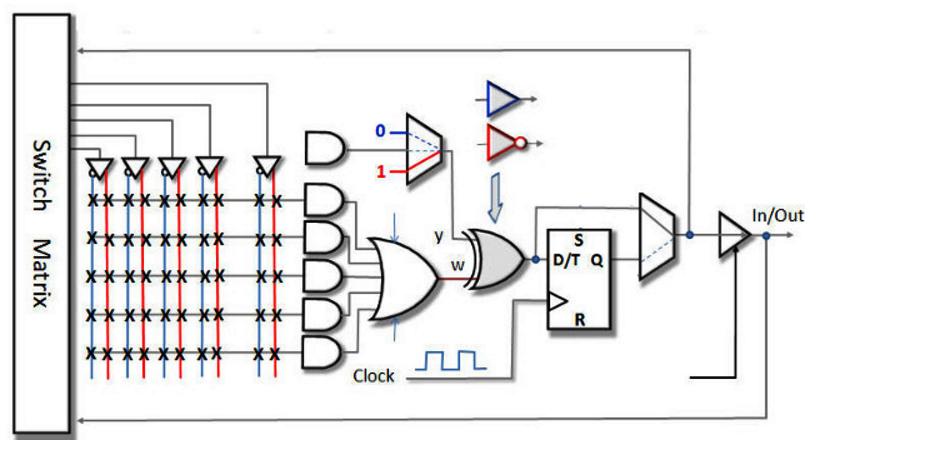
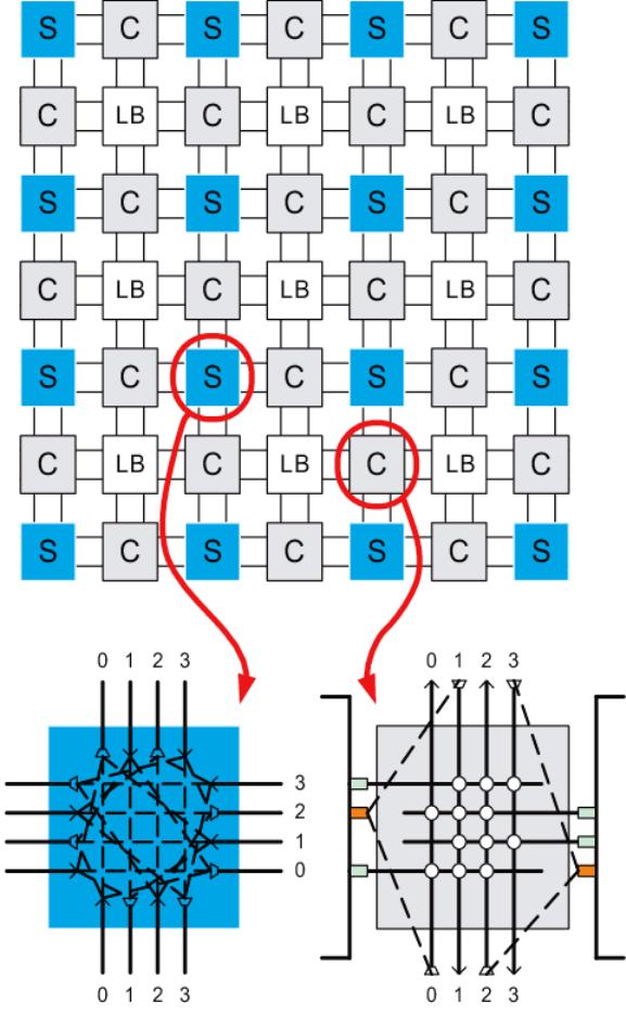
Regardless of the different manufacturers and several different architectures and feature sets, most FPGAs have a common approach. The main component blocks of any FPGA are a flexible programmable “logic block” (CLB), surrounded by programmable “I / O blocks” with a hierarchy of routing channels connecting the various blocks on the board.
In addition, they can consist of DLLs for distributing and managing the clock and RAM memory of the allocated block with the main building block of the logical cell. The latter consists of a generator of input functions, transfer logic, and storage elements. Generators are implemented as look-up tables and depend on the introduction. For example, Xilinx Spartan II has 4 input LUTs, each providing 16X1 bit synchronous RAM using multiplexers as shift registers to capture data in batch mode. Storage elements are sensitive to the edges of the triggers or to the level of the valves.
FPGA programming fragment:
- Arithmetic logic includes an XOR gate for working with a full adder and highlighting logical carry lines.
- I / O unit and routing matrix. This unit has inputs and outputs that support a wide range of standards and signaling interfaces.
The basic input / output unit is shown below.
Buffers in the input and output paths direct the signals to the internal logic and the resulting pads directly or through a trigger. They are configured to meet various supported signaling standards that can be user defined and set externally.
Routing matrix
On any assembly line, a slow segment determines overall performance. Routing algorithms are used to develop the most efficient ways to ensure optimal performance. Routing is carried out at different levels, such as local, general-purpose routing between different CLBs, I / O routing between blocks and CLBs, dedicated routing for specific signal classes in order to maximize performance, and Global Routing for distributing clock and other signals with very large branching . FPGA families also have large block RAM structures to complement distributed LUT RAMs, the size of which varies for different FPGA devices.
FPGA design assumes basically the same approach as any VLSI system, the main stages of which are design, behavior modeling, synthesis, post-synthesis modeling, translation, mapping and routing, as well as subsequent analysis, such as synchronization modeling and static synchronization analysis. On a computer, the design looks orderly and tiled, but in fact there is imperfect placement and routing, which leads to reduced performance.
To increase FPGA performance, you can always use more transistors. The office area is high. Installing more transistors means larger designs are possible. Leakage is a serious issue for FPGAs and is of interest at the same time. Using the asynchronous FPGA architecture delivers better results combined with pipelining technology that reduces global inputs and improves throughput.
Gate quality and problems
System security has always been a major concern, as the code must be opened every time it is loaded into the FPGA. Such flexibility makes FPGA a potential threat of malicious modifications in manufacturing, so encryption of bit streams came to its aid on time.
Often inexperienced designers and users are faced with a dilemma of how powerful FPGAs are suitable for their development. Manufacturers often indicate metrics, for example, “number of gates”. For example, Xilinx FPGA programming uses 3 metrics to measure FPGA capacity, maximum logic gates, maximum memory bits, and the typical range of gateways. As long as they are consistent, the migration between models is somewhat simplified, but it rarely offers exact comparisons from different vendors through variety in architectures and due to differences in performance.
The best indicator is a comparison of the type and amount of logical resources provided. In addition to this, the developer must fully understand what exactly is needed from the device, since manufacturers can boast of features that will be of the least importance for work. For example, Altera's Stratix II EP2S180 has about 1.86.576 LUTs with 4 inputs, and the Xilinx Virtex-4 XC4VLX200 contains 1.78.176, respectively. However, if only 177 thousand LUT are needed for design, this will be enough.
If RAM is a desirable metric for the designer, then neither the 6 Mbit Xilinx XC4VLX200 nor the 9 Mbit Altera EP2S180 will be preferred over the less-advertised, older 9.9 Mbit XC4VFX140.
Programming and Software Languages
Programming FPGAs Altera for beginners starts with a choice of language. The option C, C ++ or System C allows you to use the capabilities of the largest devices and, at the same time, achieve the similarity of realistic development graphics. The possibility of using C-based for FPGA design is provided by HLS (high-level synthesis), which for many years is on the verge of a breakthrough with a tool such as Handle-C. Recently, this has become a reality due to the fact that major suppliers Altera and Xilinx offer HLS in their Spectra-Q and Vivado HLx toolkits, respectively.
A number of other Altera C-based FPGA programming implementations are available, such as OpenCL, which is intended for software developers who want to increase productivity using FPGAs without a deep understanding of FPGA design.
As with HDL, HLS has limitations when using C FPGA programming approaches as well as with traditional HDLs, developers have to work with a subset of the language. For example, it is difficult to synthesize and implement system calls, since you need to make sure that everything is limited and has a fixed size. In HLS, the nice thing is that you can develop your own floating point algorithms and there is an HLS tool for converting floating point to fixed point.
Programming FPGAs with Xilinx software is not at all difficult. You can get it by purchasing Xilinx products, for free or at a price that is specific to your models. You can access the video on the profile site, which clearly shows the procedure for use. Of all the companies that you can choose when searching for programmable valve arrays, Xilinx is by far the best of all. They are the creators of this product, and over the years have made improvements to it. Proprietary software has become more powerful than ever before.
Design stages
FPGA programming training can be done online because the platform is well represented on the Internet. When setting up an FPGA, the first step is to design a circuit that requires knowledge of digital electronics. Unlike programming, it is much more difficult to start code slicing if the architecture of the program is not clear. As soon as it becomes clear what needs to be implemented, begin to describe the circuit using one of the languages: Verilog or VHDL.
The fact that indicates a paradigm shift is that they are not called FPGA programming languages, but are description languages. Due to the complexity of testing digital circuits, usually at this stage test banks are used that simulate the behavior of the equipment. This type of tool allows you to see the signal state at any time and check if there are transitions with the desired results.
The third stage is known as synthesis circuitry is one of the key. He selects the elements used and their relationship in accordance with the description files. This stage requires tools that, in most situations, facilitate and automate tasks.
Hardware and commissioning
Intel Quartus Prime Software Suite Lite Edition - FPGA Design Software. It is ideal for beginners, as it can be downloaded for free, and a license file is not required. You can download the software on the manufacturer’s website. Files are large (several gigabytes), downloading and installing them can take a lot of time. , , . , , «Select All» Quartus Prime Cyclone V .
:
- .
- Select Next> Directory> Name> top-level object.
- Choose a directory for the project, for example, “Blink” and place it in the intelFPGA_lite folder, but you can place it anywhere and click “Next”.
- When prompted to create a directory, select "Yes."
- Select "Empty project" and click "Next."
- Add files and "Next".
- Families, devices and boards are configured by choosing the following: family - Cyclone V, device - Cyclone V SE, base, device name: 5CSEBA6U2317.
- To select a specific device, you need to press the up / down arrows to see a list of supported devices until 5CSEBA6U2317 appears.
- The user may need to expand the "Name" field to see the full name of the device, click "Next".
- When setting up the EDA tool, they use standard tools, so there will be no changes, click Next and Finish. A summary screen will appear.
- Create an HDL file with the implementation of Verilog as HDL.
- Go to the File tab (main window) and select New.
- Select Verilog HDL File and press the OK button.
- Choose File> Save As.
- Choose a file name. This is the name of the top-level file, and it must match the name of the project.
- Click "Save."
- Create the Verilog module.
- Copy and paste the Verilog code below into the blink.v window, and then save the code file.
- Right-click "Analysis and Synthesis", and then click "Start" to perform syntax and syntax verification of Verilog code.
If the process completes successfully, a green checkmark is displayed next to the analysis and synthesis. If there is an error, check the syntax and make sure that it exactly matches the code block indicated above.
All experienced programmers know that complex programs, even subroutines, do not work correctly the first time. The abilities of abstraction in a person, based on experience, allow him to find solutions without worrying about the smallest details. But the harsh truth is that the physical system into which the programs are embedded requires that every little thing be taken into account before everything works.
With the improvement of software tools for FPGA development mainly from traditional suppliers, as well as independent tool suppliers: Synplicity, FPGA - it is becoming more and more popular day by day. Now FPGAs have begun to include specialized hardware for the functions necessary for the client, reducing the costs of manufacturers. Thus, in the future there may be competition between hard and cheap systems with flexible cores. It is expected that in the near future costs will decrease even more, as the popularity of FPGAs will increase at times.
Manufacturers began experimenting with a concept such as embedding FPGAs in integrated circuits to create a hybrid device. The focus is still on interconnect routing, and smaller changes are seen in CLB architectures. As FPGAs continue to include processors, the new generation will require not only knowledge of digital design hardware, but also the experience of developers in the process of programming FPGAs once. Overall, FPGAs are expected to take market share in ASICs and become the dominant technology spanning many applications from a variety of fields.